
© © 2025 Copyright © Youibot Robotics Co., Ltd. All rights reserved.SitemapPrivacy Policy
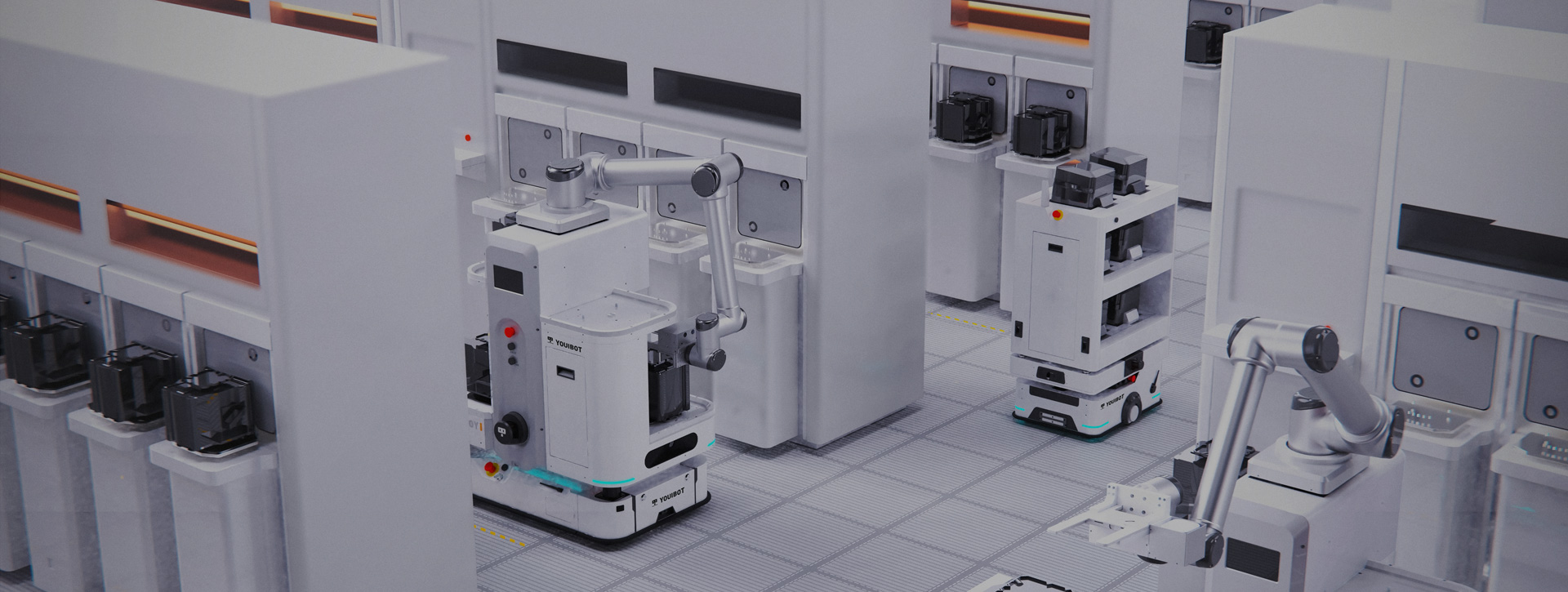


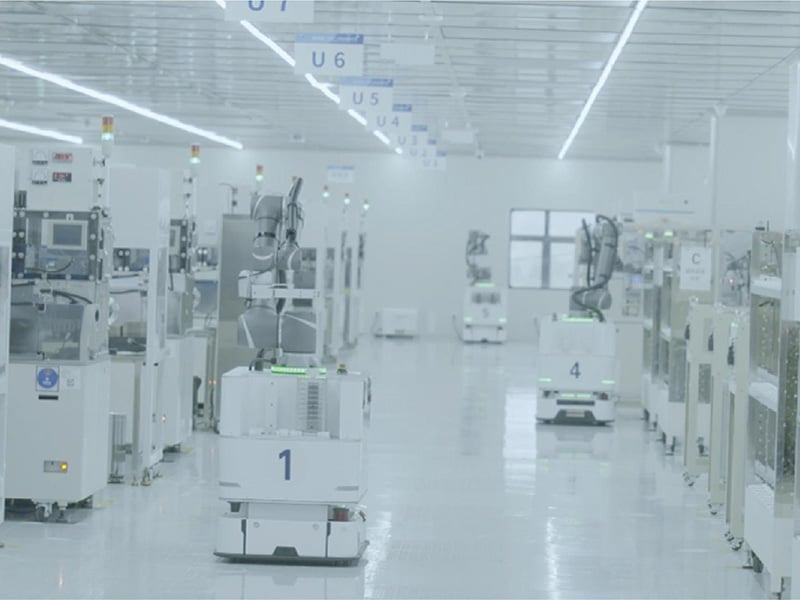
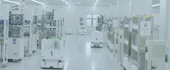
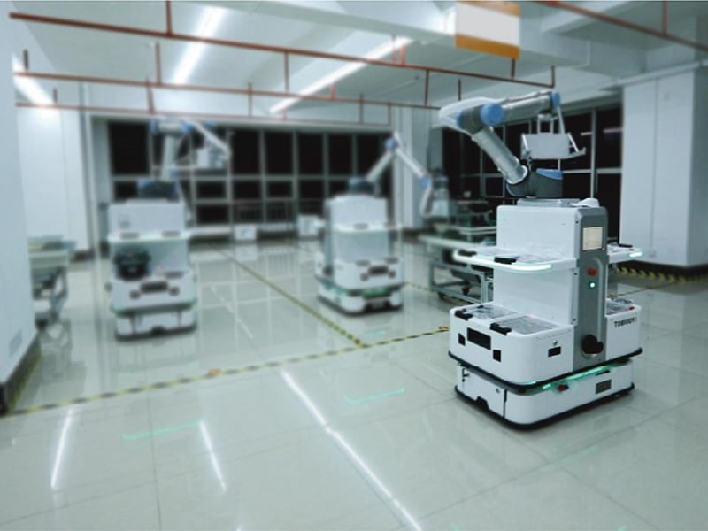
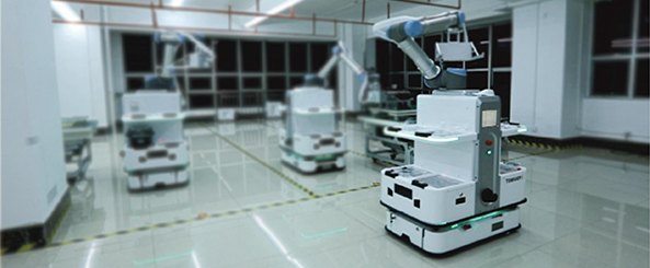
Aiming at the problems of inefficiency, human error and contamination risk in the internal logistics of the semiconductor industry, Youibot proposes the robot solution. Our material handling robots and mobile manipulators aim to connect the material flow and information flow between different processes, realizing automatic wafer transfer or automatic loading and unloading of materials in every workshop and manufacturing equipment. It dramatically improves semiconductor production efficiency and realizes seamless human-robot collaboration through the joint operation of cobots, such as automated material handling robots and mobile robotic platforms with robotic arms.
As an industry-leading collaborative robotics company, we continue to explore the latest robot technologies, accumulate a wealth of successful cases, and build material handling robots that are widely recognized. These semiconductor composite robots can solve the problems of low efficiency and low product yield caused by manual operation.
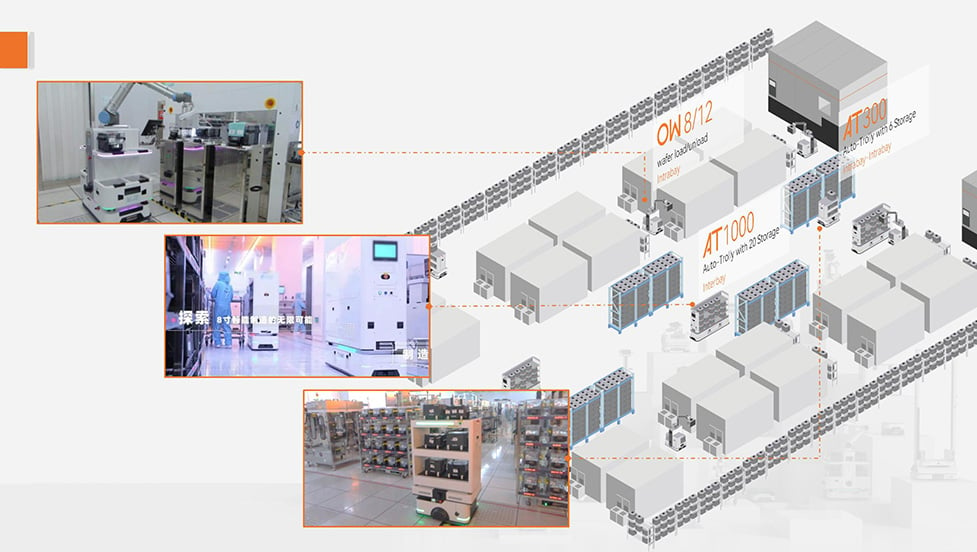
The O series of collaborative robots are custom designed for vaious materials handling scenarios in the semiconductor industry.
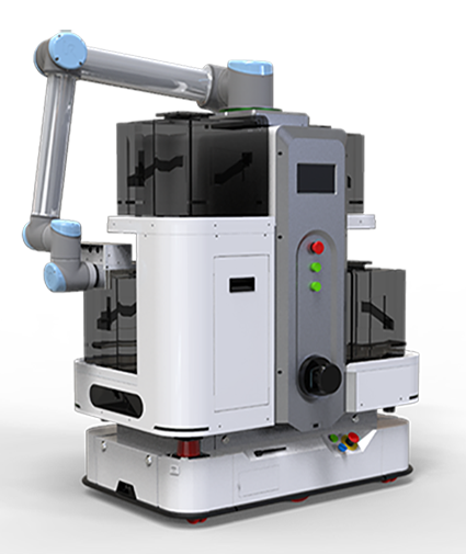
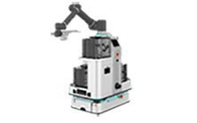
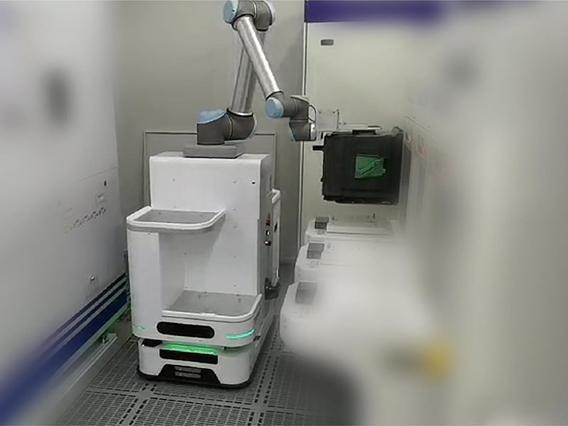
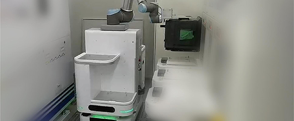
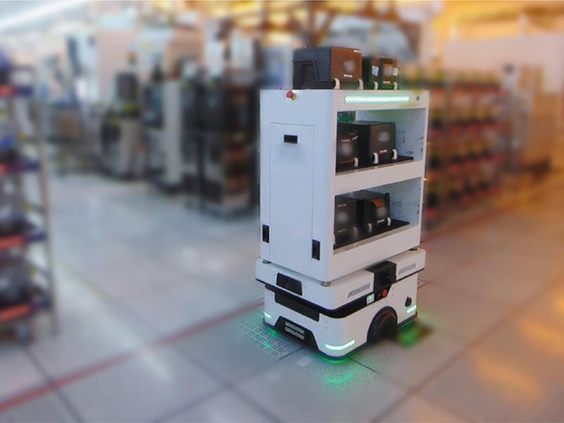
Youibot OW12 is a mobile manipulator designed for loading and transferring 12'' Foup pods, which is helpful for semiconductor manufacturing automation.
See More >>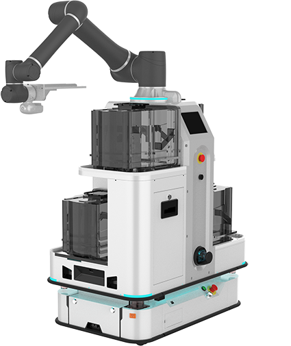
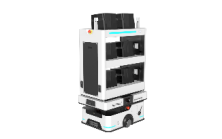
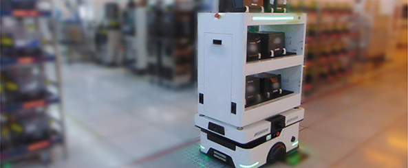
Youibot OW8 is a mobile manipulator equipped with cobot. It offers an automation solution specialized for loading and transferring the 8'' Foup Pods.
See More >>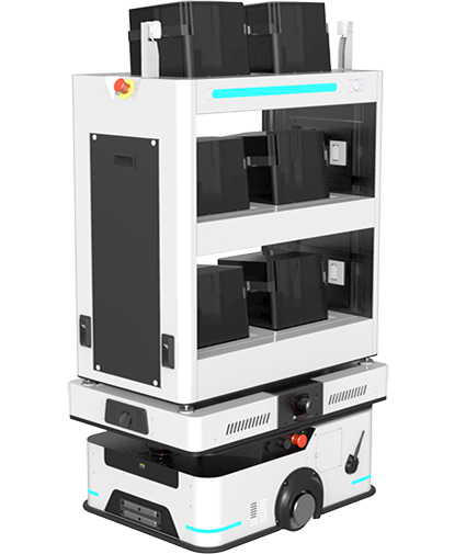
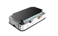
Youibot ATS is a robot designed for transfering FOUP pods in the semiconductor industry. Its flexible configurations can be customized to meet specific operational needs.
See More >>

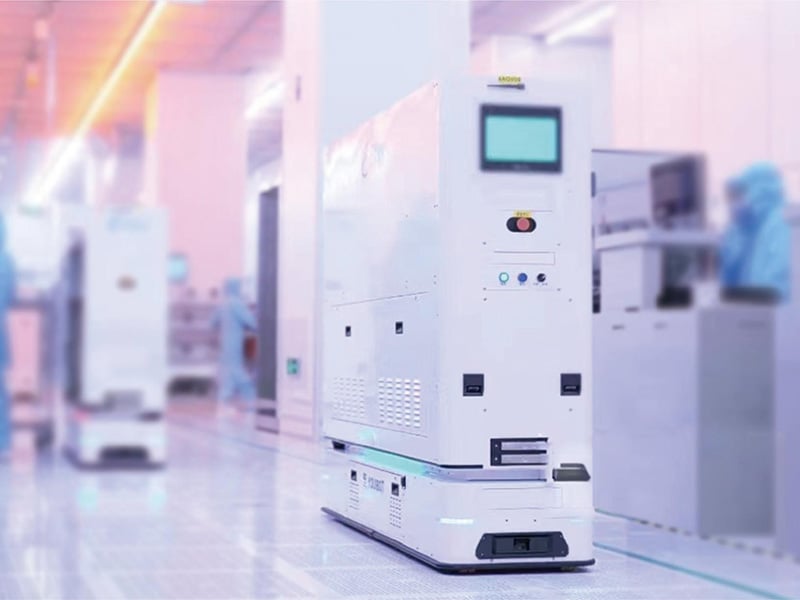
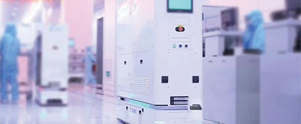
Due to smooth and contamination-resistant surfaces, the semiconductor robot meets a high cleanliness level. It minimizes human intervention, thus reducing the risk of contamination and increasing the product yield rate.

Robots can run uninterruptedly for a set period of time. It enables automatic transfer or automatic loading and unloading of materials and intelligently navigates through complex environments without the need for human intervention or fixed tracks. This ensures a smooth production process to increase capacity.

The robot, equipped with advanced vision sensors and an end gripper with strong control, grasps the FOUP PODs precisely, reducing direct contact with the wafers and minimizing vibration effects on the raw material.

Automated handling replaces some of the labor requirements. It not only reduces long-term labor expenses but also greatly avoids manual errors. Such cost reductions and efficiency enhancements help to realize a quick return on investment.

The integrated robot control system seamlessly integrates the robot's upper system and various end-sensing control systems into the internal operating system, reducing the cost and time of switching between multiple systems during deployment. Workflow and logging make all operations traceable and reduce management hassles.

The robot's built-in SLAM algorithms help it locate its position and direction on a map to create a logical route of movement. It can also safely avoid obstacles in complex environments to safeguard personnel and equipment.

F Company, a leading semiconductor firm, upgraded the logistics automation in their packaging and testing workshop.
non-stop operation
Vibration value during transportation
F Company, a leading semiconductor firm, upgraded the logistics automation in their packaging and testing workshop.
Twelve robots were deployed to automate the loading and unloading processes in the packaging and testing area.
High Efficiency: Each robot performs 215 tasks daily, handling 1,070 trays with an average distance of 9,675 meters.
Scalable Automation: The 12 robots collectively execute 2,580 tasks, handling 12,840 trays and covering 116,100 meters each day.
T Company, a global semiconductor leader, enhances production efficiency
and reduces labor costs with Youibot's automated wafer handling solution.
employees labor shortage solved
materials moving daily
T Company, a global semiconductor leader, enhances production efficiency and reduces labor costs with Youibot's automated wafer handling solution.
23 Youibot robots operate in a loop across 12 Intra Bays, transporting SMIF Pods.
Each robot has 20 storage slots, making the solution 3-4 times more efficient than manual handling and 5 times more efficient than OHT.
Company S's 8-inch wafer workshop faces accuracy issues due to high operator turnover. AMR solutions are deployed to improve consistency.
mixed-site scheduling
materials moving daily
Company S's 8-inch wafer workshop faces accuracy issues due to high operator turnover. Robot solutions are deployed to improve consistency.
80+ wafer handling robots (OW8) automate material loading/unloading, filling gaps in manual transport tasks.
80+ Robots handle 32,000 FOUPs daily, alleviating labor shortages and enabling 24/7 operations with mixed-site scheduling and 7 robot types.
H Company’s project aimed to upgrade the logistics automation of a high-cleanliness 12-inch wafer processing workshop, which operates as a Class 10 cleanroom and requires equipment to meet ISO Class 4 standards.
daily tasks executed
cleanroom automation upgrade
H Company’s project aimed to upgrade the logistics automation of a high-cleanliness 12-inch wafer processing workshop, which operates as a Class 10 cleanroom and requires equipment to meet ISO Class 4 standards.
Five Youibot robots were deployed, to enhance automation within this high-cleanliness environment.
High Cleanliness Compliance: Youibot robots are engineered to operate within ISO Class 4 standards, supporting the Class 10 cleanroom requirements.
Enhanced Automation: Improves efficiency and accuracy in wafer handling and processing, adhering to stringent cleanroom standards.
S Company, a leading semiconductor firm, sought to automate logistics for 8-inch wafer transportation across factory buildings.
daily material transfers
vibration level during transport
S Company, a leading semiconductor firm, sought to automate logistics for 8-inch wafer transportation across factory buildings.
Twelve robots were deployed to manage cross-building logistics, featuring Youibot's ATS6 robots with vibration-damping storage and advanced Fusion SLAM algorithms to handle complex environments and sensitive wafer transport.
Cross-Building Automation: Efficiently automates wafer transportation between buildings.
Vibration Control: Ensures vibration levels are below 0.1g, protecting delicate wafers and enhancing production quality.
High Throughput: Handles 6,972 material transfers daily, optimizing logistics efficiency.

By continuing to use the site you agree to our privacy policy Terms and Conditions.